PCB Design · Digital · DU IEEE
IEEE LED Matrix Cube Board
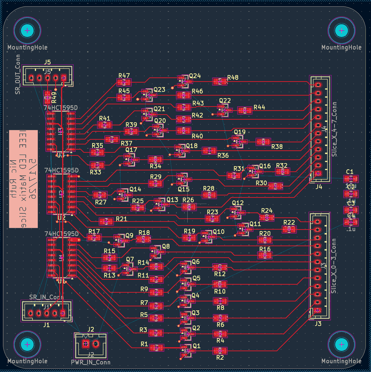
- Role
- One slice of the chapter's LED matrix cube
- Drivers
- 3 × 74HCT595D shift registers, daisy-chained
- Channels
- 24 (eight columns × red, green, blue)
- Switching
- MMBT3904 NPN low-side sinks, 2.2 kΩ base resistors
- Ballast
- 68 Ω on blue and green, 120 Ω on red
- Control bus
- Five wires: CLK, DATA, LATCH, BLANK, GND
- Tool
- KiCad
Eight RGB columns, five wires
An LED cube needs a huge number of separately controlled outputs, and a microcontroller doesn't have nearly enough pins. The solution is to clock the LED states in as serial data instead of driving each one from its own pin.
Three 74HCT595 shift registers sit in series. Each one takes serial
data on one pin and presents eight parallel outputs, so three of
them give 24 outputs, which is eight columns of red, green, and
blue. The processor shifts 24 bits in on DATA and
CLK, pulses LATCH, and the whole slice
updates at once.
The fifth signal, BLANK, drives the registers' active-low
output-enable pins together. It turns every output off at
once without changing the latched data, so it works as a
brightness control. Driving it with PWM dims the whole slice
without changing the frame.
Why red gets the bigger resistor
The shift register outputs can't sink enough current for an LED, so each of the 24 channels drives an MMBT3904 through a 2.2 kΩ base resistor and the transistor sinks the current. The ballast resistors took more thought.
Blue and green LEDs drop roughly 3 V; red drops closer to 2 V. With all three on the same 5 V rail through the same resistor, the red channel would get much more current than the others, so the cube's “white” would look pink and the reds would burn out sooner. Using 120 Ω for red and 68 Ω for blue and green brings the three currents into the same range so the colors mix properly.
Built to chain
The board is one slice of a larger cube, so its five-pin output
header mirrors its input header exactly: the last register's
overflow output becomes the next slice's DATA, and
clock, latch, and blank pass straight through. Slices stack without
any wiring changes, and the firmware just shifts in a longer
frame.
That overflow line goes out through a 68 Ω series resistor. The data line has to make it through a ribbon cable to the next board, and the resistor damps the reflections that fast CMOS edges cause on an unterminated line.
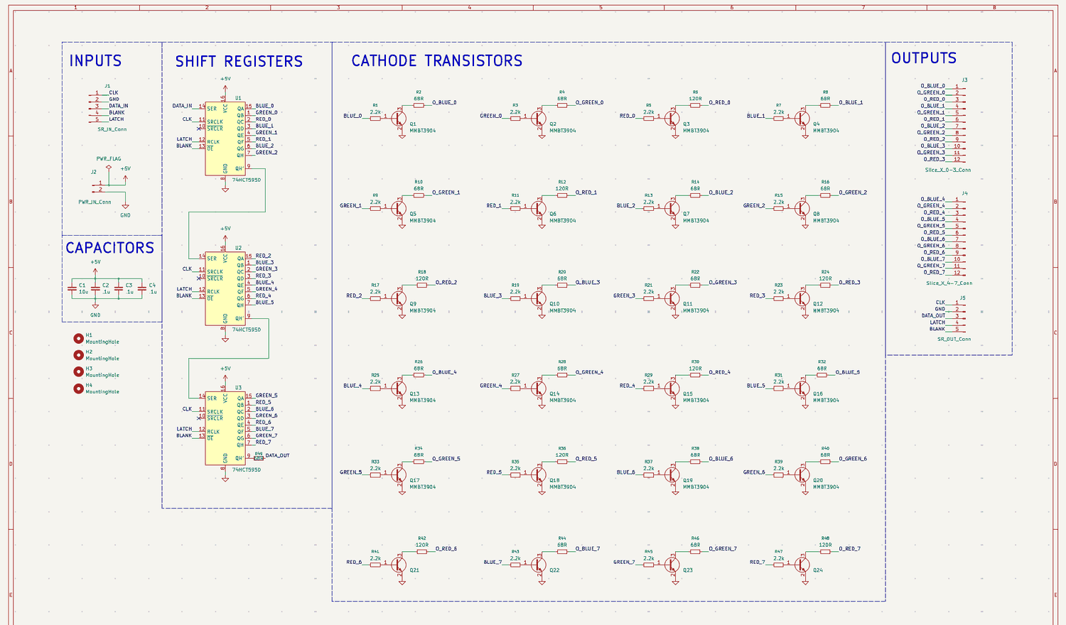
Designed with the University of Denver IEEE student chapter. This board is the layout for one slice, and the full cube is the chapter's group project.